Potential Barrier In Pn Junction Diagram
Explain with the help of a diagram the formation of depletion region Pn junction operation Junction pn barrier operation formation diodes basic electronics
What is PN Junction - The Engineering Knowledge
Junction pn diode formation symbol characteristics region barrier drift formed depletion potential diffusion type electric field built electrons holes biasing Barrier potential height pn junction energy diagram band Potential barrier diode junction pn define regards
Depletion diode discuss
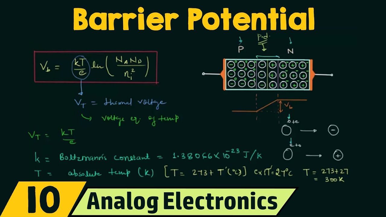
In a p–n junction there exists a barrier potential. fig. (a) shows theJunction pn depletion barrier conduction valence Potential barrierHow is pn junction formed? basics and examples.
Junction barrier connected batteryPotential built junction pn calculation What is pn junctionIn figure, v0 is the potential barrier across a p-n junction, when no.

Junction energy bias field biased potential electrostatic transition region electric effects
Pn junction diode – formation, symbol, biasing, v-i characteristicsDefine barrier potential for pn junction diode What is pn junctionJunction formed depletion.
Junction biased effectExplain the formation of potential barrier in a p What is meant by height of potential barrier ? (energy band diagram ofBarrier potential.

Barrier potential junction depletion region diagram explain formation help pn positive diode cycle half class physics conducts corresponding working does
Barrier junction exists sarthaks correct biasing第三周之3 calculation of built in potential of pn junction 19. pn-junction — modern lab experiments documentation.
.